Before reading this post I highly recommend that you pay a visit to Mike’s Electric stuff webpage where Mike describes the reverse engineering of the Ipod Nano 6th gen LCD. It it essential to have at least some understanding of how it works since Ipod 7 LCD (IP7 for short) does it’s job in a very similar manner.
Pinout
IP7 LCD shares the same connector with IP6 LCD, but the pinout is different. Since I do not posses IP7 I had to come up with a way of determining the pinout using a little bit of diode tester trickery. Both LCDs have 12 pins so we can assume that signals will be the same – only difference being their pin positions.
We build a list of pins to find: backlight LEDs (anode, cathode), supply (1.8V, 3.0V), logic signals (clk-, clk+, dat-, dat+, nrst, sync), ground.
Ground pins can be identified almost instantly: just check the continuity between all of the 12 pins and the metal piece covering the plug. Four corner pins in the connector are also connected to ground so you can use these for convenience (no need to probe things from two sides of the connector).
Rest of the pins can be identified using diode tester and knowing that all digital and supply pins are ESD protected (using internal diodes):
Backlight LEDs are not referenced to anything (anode is floating, cathode is not grounded so that it can be used in boost converter feedback loop to measure LED current). These are easy to find: Put your meter in diode tester mode, attach positive probe to connectors ground: there should only be two pins without a diode from ground to that pin: anode and cathode of the LED backlight string. These are Anode – pin 8, Cathode – pin 10.
Now let’s find 3.0V power supply. This supply rail is not used in the digital domain so there should be no ESD diodes present from any signals that are left (logic and 1.8V) to this supply rail. The only ESD diode present should be from the ground. This is in fact Pin 12.
1.8V logic supply is the one that all of the remaining logic signals have an ESD diode clamped to. So put the negative probe of your diode tester on the pin that you suspect to be the 1.8V rail and probe all of the remaining pins (logic signals). If all show a diode drop – voila! you’ve successfully located the 1.8V supply pin, if not – move the negative probe to the next pin a start all over. Pin 2 – is the correct guess.
All of the remaining pins are logic signals. The diode tester method does not help in determining the pin function, but some assumptions can be made: Clock and Data both use differential pair signalling so their positive and negative pins need to be close to each other. Since these are high-speed then we can expect a ground connection nearby. Pins 1,3 – are the first diff pair, Pins 7,9 are the second. We do not know which one is clock or data, we do not know which one is positive/negative – so that leaves us 4 combinations to try out during FPGA developement.
Reset and Sync (Pins 4, 6) are both “low speed” signals, reset being an input and sync being an output. Since we do not know yet which one is which it would be wise to connect both to weak pull-ups. That way we don’t blow up the Sync output and we keep the reset disabled (reset is active negative).
Pin numbering:
Final pinout:
| Pin Number | Pin Name | Description |
|---|---|---|
| 1 | CLK_P | Clock lane (positive) |
| 2 | VDIG (1.8) | Logic supply rail |
| 3 | CLK_N | Clock lane(negative) |
| 4 | Reset | Active low (in 1.8V domain) |
| 5 | GND | Ground |
| 6 | SYNC | Vertical Sync pulse |
| 7 | DAT_P | Data lane (positive) |
| 8 | LED+ | LED anode(consumes around 20mA @ 14.7V) |
| 9 | DAT_N | Data lane (negative) |
| 10 | LED- | LED cathode |
| 11 | GND | Ground |
| 12 | VLCD | 3.0V supply |
Preparing the Lattice MachXO2 board
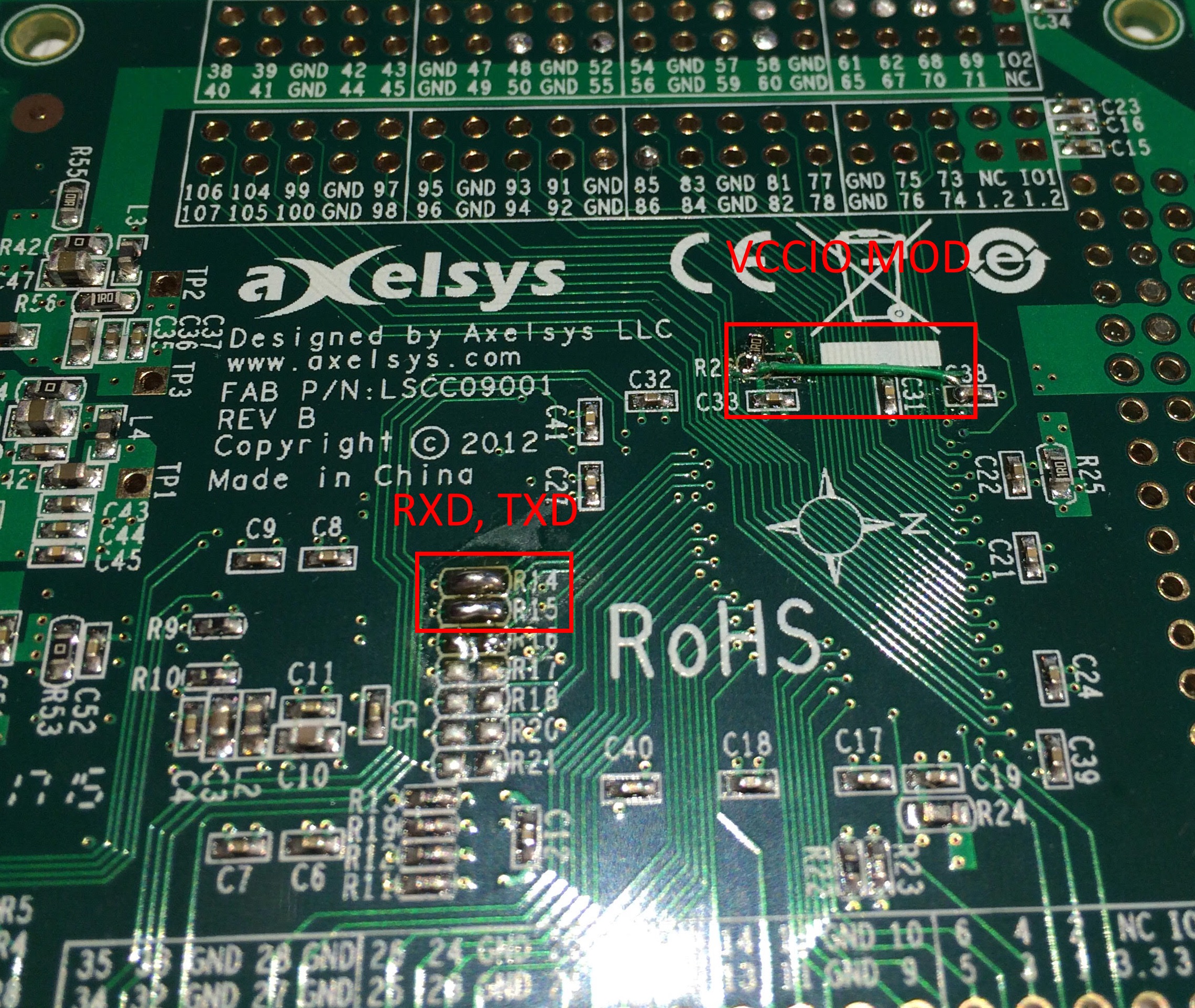
First of all change the power supply voltage (VCCIO) of the FPGA IO bank that you wish to use for logic signals. You don’t want to push 3.3V signals into 1.8V domain. I took the liberty and reconfigured the Bank 2 supply by removing the R26 and soldering a jumper wire from the nearest 1.2V FPGA core supply (one of the C38 pins, easy to identify, the other one is ground). 1.2V sound a little bit on the low side, but this is actually desirable since MIPI DPHY asks for 1.2V signalling during low power states. Reset and Sync also seem fine about 1.2V.
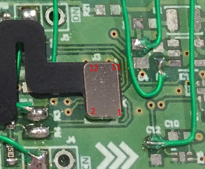
If you are planning to use UART as the external image data source (in the end we need to have something to display, right?) as I did make sure that the FTDI chip is configured for UART operation (can be done with FTDIProg, important step: the default mode is SPI, I think) and solder bridge two connections: R14 and R15 – this will connect RXD and TXD lines to FPGAs pins 73, 74 respectively.
Here is a photo of the mod:
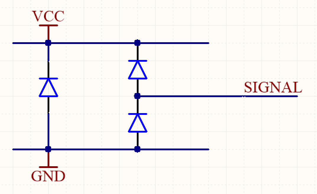
Since MIPI DPHY mixes the low-power (full 1.2V swing) with high-speed (LVDS) signalling it is necessary to add external resistors to the fpga output pins. Please follow the diagram (keeping in mind that this is all for 1.2V):
For details regaring which FPGA pin is connected where please see the FPGA configuration file. Just to clarify: reset is the display reset, nrst is the FGPA reset (currently not used).
Communication between FPGA and Display
The communication is the same as with IP6 display. Please see Mike’s Electric stuff webpage for details. One thing to note: I was able to make the Set Line Address / Set Column Address commands to work. These in fact care about the CRC value. One might find these commands handy for low speed/low mem systems when one wants to refresh only a part of the screen. If you want to know how to compute the CRC then take a peek at my source code repository for this project.
I’ve provided the Verilog code for this project to be used with Lattice Diamond. FPGA takes care of the Low Power -> High Speed transition as well as sending the initial 0xB8 byte on the data lane. FPGA listens to incoming UART bytes (2766400 bauds, 8N1) that are SLIP encoded. I used SLIP to encapsulate raw byte stream into frames and the framing signal itself is used to start/stop the communication over Data Lane/Clock Lane.
MIPI DPHY requires that the clock signal is in quadrature with the data bits so that the receiver (display) has the best setup/hold conditions. Quadrature clocks are easy to generate with PLL but since I am planning on implementing this solution on low end FPGA I went for a different approach. I used the LUT as a delay element and routed the Clock Lane clock through it. That gave me couple of nanosecods of additional delay – and which did the job. Take a look at this file for details.
Serializers were done around simple DDR output flip flops, no 8:1 gearing was used – all to allow reusing the code on a cheap-o programmable logic.
Communication between PC and FPGA
PC sends SLIP encoded binary data over UART. Data is just MIPI DSI commands. All the CRCs ECC and other stuff are calculated by PC. The source code is available here. Requires node.js. Code takes care of the display initialization and sends three test bitmaps in a loop creating a nice slideshow.
One thing that I’ve noticed: there is a timeout on MIPI DPHY which means that one cannot sent frames that are too long (meaning > 50ms). That dictates that we split the bitmap sending into couple different frames.
Here’s the overall outcome: