Antminer S1 is the 1st generation of Bitcoin mining hardware based on Bitmain Technologies chip marked as BM1380. There are 64 chips (2 boards, 32 chips each) per miner offering hash rates at around 120GH/s under normal conditions. In this article I present my approach at reverse engineering the communication protocol the chips use in order to make them do some actual work (i.e. mine some Bitcoins). At the time of writing this post were clearly much more powerful mining rigs available making the S1 pretty much obsolete, which makes for a perfect opportunity to acquire the S1 for next to nothing.
If you, Dear Reader, are feeling generous and might find my writing beneficial, then feel free to donate some BTCs: 152dEicovRXbxBgTmoY3izd7ThrxRNdPqW Much obliged!
BM1380
First of all: the datasheet gives very little information about how this chip actually works (I imagine that more detailed specification is available for those that buy these in large quantities). Schematics of S1 reveal information about the functionality of certain pins.
Chips in S1 use UART for communication, settings are 115200, 8N1. Chips communicate within the chain using UART + flow control signals:
- CI – Command Input <-> uplink’s (like a control board, or so) TXD
- RO – Response Output <-> uplink’s RXD
- CO – Command Ouput <-> connected to CI of the downlink (meaning: next chip in chain)
- RI – Response Input <-> connected from downlink’s RO
All of the chips are basically sharing the same UART “bus”. Flow control/bus arbitration is done using BI (Busy Input)/BO (Busy Output) signals. Chip that wants to send the data out activates it’s Busy Output signal which mutes all chips that are placed further in chain.
Chips have addresses derived from the state of address pins ADDR[7:0] which also determine the MSB value of starting ‘nonce’. S1 has these equally spaced like 0x00, 0x08, 0x10 … 0xf8, so that each chip covers different (and equal in size, 0x07FFFFFF) area of nocne value search.
One can see that the pinout is really optimized for daisy chaining. Single hashing board of S1 uses only one crystal oscillator, all other chips derive their clocks from preceding chips in the chain. Even the Reset signal is chainable.
Operation
Chip is ready for work just after powering up (no need for any form of initialization if you are happy with default clock frequency of 193MHz). Chain awaits for 64 bytes of work data after which it stars searching for a valid nonce. Chips report nonces that result in hashes with at least 32 leading zeros. There might be more than one such nonce in the whole 2^32 nonce search space, but there may be none as well.
Chip report results in the form of 5 byte UART messages only if a valid result is found. No messages will be emitted if no valid nonces were found. Because of that it is essentinial (from the performance point of view) to know how much time it is needed for the chain to do the full nonce search and after that time has passed we need to switch to the new work as soon as possible.
Sending work data interrupts current work and restarts the whole nonce search. No other signalling is needed in order to make the chips work on new data. Chips start to look for valid nonce beginning at starting nonce which is configured using address signals.
Communication
There are two types of messages that chips recognize:
- Commands – 4 byte messages ended with CRC. Valid CRC is crucial – chips interprets data as commands only if CRC is ok.
- Work vectors – 64 byte messages that contain all the information needed for hashing units
Not every command/work vector will result in response. Every response is always 5 byte long which eases the processing. Command responses differ from Nonce Responses by the CRC5 (of course certain nonce values may produce Nonce Responses that pass the CRC5 check so it’s not the reliable way of determining whether the response is caused by command or Work Vectors).
Commands
Format resembles what can be found in BM1385 datasheet, which means that not a whole lot has changed over time. Generally all commands follow the same frame format:
| Byte 0 | Byte 1 | Byte 2 | Byte 3 | ||
|---|---|---|---|---|---|
| [7] | [6:0] | [7:0] | [7:0] | [7:5] | [4:0] |
| ALL – broadcast command to all chips (if set) | CMD – command code | command parameter 1 | command parameter 2 | reserved (zeros) | CRC5 computed over first 27 bits |
Read Register
Command useful for determining the length and addressing of the chips that build up the chain as well as making sure that PLL settings are applied as requested. Produces 5 byte responses that return the value of the register being read. Broadcasting (using ALL bit) causes every single chip to produce response of its own. PLL status register carries scrambled bits of frequency code words (bits in table use the same notation as in Set Frequency command)
| Read Register | |||||
|---|---|---|---|---|---|
| Byte 0 [7] | Byte 0 [6:0] | Byte 1 [7:0] | Byte 2 [7:0] | Byte 3 [7:5] | Byte 4 [4:0] |
| ALL – broadcast command to all chips (if set) | 0x04 – Read Register | Destination address, don’t care if ALL is set | Register address | reserved (zeros) | CRC5 computed over first 27 bits |
| Read Register Response (reading register 0x00 Device Address) | ||||
|---|---|---|---|---|
| Byte 0 | Byte 1 | Byte 2 | Byte 3 | Byte 4 |
| – | – | – | device address | CRC5 computed over first 27 bits |
| Read Register Response (reading register 0x04 PLL status) | ||||
|---|---|---|---|---|
| Byte 0 | Byte 1 | Byte 2 | Byte 3 | Byte 4 |
| aa00 0000 | 0aab bbbc | 000c ccdd | 0000 00dd | CRC5 computed over first 27 bits |
Set Frequency
Command used to set the operating frequency. Has a direct impact on hashrate. Can drive the ICs into self-destruction if no proper heatsinking is in place. Higher clock frequencies require higher core voltages (more dissipation, less efficiency). Chips are happy with only 0.8V of core voltage for nominal operating frequency of 193MHz, pushing the clock any further results in much more errors (nonces that don’t produce hashes with at least 32 leading zeros) being reported, making the overclocking profitability (without rising the core voltage) questionable. Does not provide a way to address a single chip from the chain (not that useful when you think about it), so it only makes sense to use it with ALL bit set.
| Set Frequency | |||||
|---|---|---|---|---|---|
| Byte 0 [7] | Byte 0 [6:0] | Byte 1 [7:0] | Byte 2 [7:0] | Byte 3 [7:5] | Byte 4 [4:0] |
| ALL – broadcast command to all chips (set) | 0x02 – Set Frequency | MSB of FreqWord | LSB of FreqWord | reserved (zeros) | CRC5 computed over first 27 bits |
I wasn’t able to get the full picture of certain parts of frequency coding words, still one can easily see that ‘bbbb’ bits make for the PLL’s VCO divider – increasing it’s value by two results in a clock faster by twice the REFFREQ (25MHz from crystal) Different coding for 193MHz must result in PLL using some prescaled version of 25MHz reference clock. Bits denoted as ‘dddd’ drive the output divider giving following ratios: 0x1 – /1, 0x2 – /2, 0x3- /4, 0x 7 -/8, 0xF -/16 – so you can go very slow (useful for developement). Here are a couple of “popular” frequency settings.
| Frequency Words | |
|---|---|
| 16-bit Word (aaaabbbbccccdddd) | Frequency [MHz] |
| 0x0381 | 100 |
| 0x0581 | 150 |
| 0x4F02 | 193 (default) |
| 0x0781 | 200 |
| 0x0981 | 250 |
| 0x0B81 | 300 |
| 0x0D81 | 350 |
| 0x0F81 | 400 |
It seems essential that Set Frequency command is followed by a Read Register with reg address of 0x04. Doing otherwise results in chip being unstable (Few chips in chain stopped reacting to commands).
Chain Inactive
Deactivates chaining which results in only the first chip being operational. Did not find an easy way out from this state (except from reset/power-cycling). Might be useful for testing purposes. No addressing mechanism is found, so after issuing you are always left with the first chip in chain. Not very useful for normal operation.
| Chain Inactive | |||||
|---|---|---|---|---|---|
| Byte 0 [7] | Byte 0 [6:0] | Byte 1 [7:0] | Byte 2 [7:0] | Byte 3 [7:5] | Byte 4 [4:0] |
| ALL – broadcast command to all chips (set) | 0x05 – Chain Inactive | – | – | reserved (zeros) | CRC5 computed over first 27 bits |
Work Vector
64 bytes that provide data for the chain to work on. Chips start cranking nonces immediately after whole 64 bytes are sent. All previous computations will be discarded. No CRC is included. Midstate and Job Data fields are byte reversed (not bit-reversed).
| Work Vector | ||||
|---|---|---|---|---|
| Byte 0-31 | Byte 32-50 | Byte 51 [7:5] | Byte 51 [4:0] | Byte 52-63 |
| Midstate (byte-reversed) | Reserved (zeros) | Reserved (zeros) | Work ID | Data (bytes 64-75 from block header, byte-reversed) |
Work ID is used for pairing Nonce Responses with Work Vectors, you can choose any number that fits in this field, it will simply be copied to Nonce Response.
Nonce Response
Emitted every time a valid nonce is found.
| Nonce Response | ||
|---|---|---|
| Byte 0-3 | Byte 4 [7:5] | Byte 4 [4:0] |
| Nonce (little-endian) | Reserved | Work ID as in Work Vector |
CRC5 Algorithm
Found that in cgminer/bfgminer source code. Here’s the javascript approach, data – Buffer, len – number of bits to compute the CRC over:
/* compute crc5 over given number of bits */
function CRC5 (data, len)
{
	var i, j, k, index = 0;
	var crc = 0x1f;
	/* registers */
	var crcin = [1, 1, 1, 1, 1];
	var crcout = [1, 1, 1, 1, 1];
	var din = 0;

	/* push data bits */
	for (j = 0x80, k = 0, i = 0; i < len; i++) {
		/* input bit */
		din = (data[index] & j) != 0;
		/* shift register */
		crcout[0] = crcin[4] ^ din;
		crcout[1] = crcin[0];
		crcout[2] = crcin[1] ^ crcin[4] ^ din;
		crcout[3] = crcin[2];
		crcout[4] = crcin[3];
		/* next bit */
		j >>= 1, k++;
		/* next byte */
		if (k == 8)
			j = 0x80, k = 0, index++;
		/* apply new shift register value */
		crcin = crcout.slice(0);
	}

	crc = 0;
	/* extract bitmask from register */
	if (crcin[4]) crc |= 0x10;
	if (crcin[3]) crc |= 0x08;
	if (crcin[2]) crc |= 0x04;
	if (crcin[1]) crc |= 0x02;
	if (crcin[0]) crc |= 0x01;

	return crc;
}
Connecting to S1 board
S1 hashing boards use 2mm connectors for control signals (connector marked as CTRL) but I found that standard jumper cables (2.54mm) can be used for attaching USB<->UART dongle. They just need to be squished a little so that they grip the connector pins. Here’s the picture:
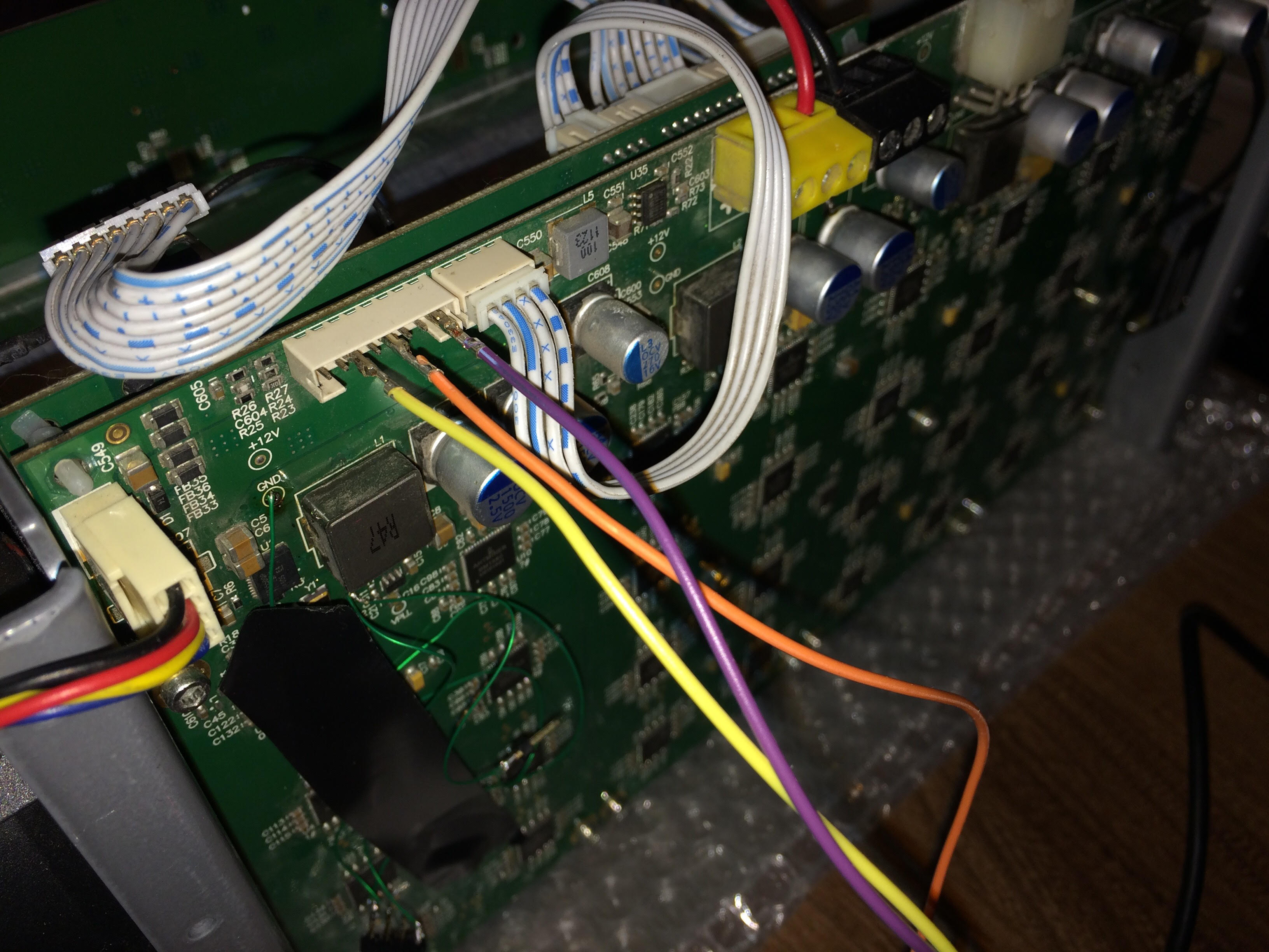
Wire colors are:
- Yellow – dongle’s RXD
- Orange – dongle’s TXD
- Purple – GND
Testing the connection
Probably easiest way to do it is to use a terminal and send out the Read Register command (0x84, 0x00, 0x00, 0x11 <- I took the liberty and precomputed the CRC).
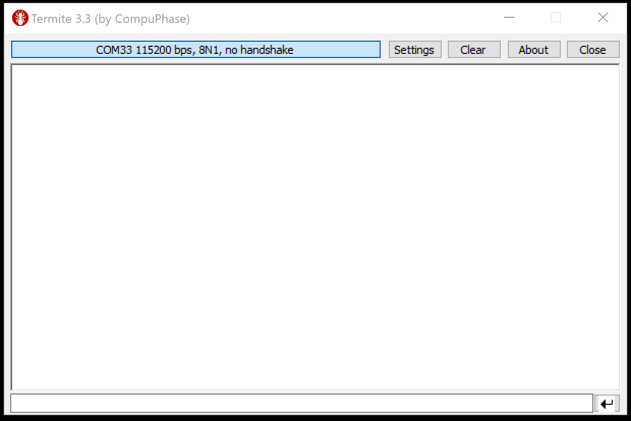
You can clearly see that all the chips from the chain have reported their addresses (4th byte of every 5 byte response).
Mining Software
Since I’ve gathered all the information needed to put these chips to use I’ve developed a simple piece of software in node.js that communicates with the mining pool (using Stratum), gets the work, prepares the work vectors, receives nonce responses, checks them against current pool’s difficulty and submits all the nonces that pass the check. Github repo is available here.
All done around Duplex streams for the sake of simplicity. The code was tested in the following environment:
- 1st hashing board was driven with miners own control board (OpenWRT + busybox + cgminer) (worker name: test)
- 2nd hashing board was connected via USB<->UART dongle (STM32 Nucleo Board to be exact, it has the UART pins located near the SWD) from my laptop. (worker name: test2)
Both boards produced the same hash rate (no noticable difference over time). Pool I used was slushpool.
